Via stitching: covering a ground plane with vias using KiCad's Python API
Place hundreds of GND vias on a ground plane by script while avoiding the mounting holes: pitch, clearance, with pcbnew or the IPC API.
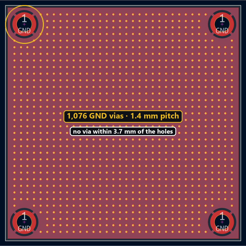
Via stitching ties the top and bottom ground planes together with a forest of vias: shorter return paths, less noise, better shielding. KiCad has no built-in tool to place hundreds of them at once. This script does it, automatically keeping clear of the mounting holes. All the code was run on a real KiCad 10 board: 1,076 vias, DRC at 0 violations and 0 unconnected items.
The idea
- A regular grid at the chosen pitch (here 1.4 mm), centred on the board.
- Skip any point too close to a mounting hole (here 3.7 mm: the pad radius plus a margin).
- Place a GND via on every remaining point.
The widget runs exactly the same computation: play with the pitch and the clearance to see how many vias fit.
Computing the points
import math

CX, CY, SIZE, PITCH, GUARD = 115.0, 105.0, 50.0, 1.4, 3.7   # mm
d = SIZE / 2 - 4.0
holes = [(CX + sx * d, CY + sy * d) for sx in (-1, 1) for sy in (-1, 1)]

n = int((SIZE - 2 * 1.6) / PITCH)          # 1.6 mm margin from the edge
start = -n * PITCH / 2
points = [(CX + start + i * PITCH, CY + start + j * PITCH)
          for i in range(n + 1) for j in range(n + 1)]
points = [(x, y) for x, y in points
          if all(math.hypot(x - hx, y - hy) > GUARD for hx, hy in holes)]
This part doesn’t depend on any API: it’s plain Python.
Placing the vias
import pcbnew

board = pcbnew.GetBoard()
gnd = board.FindNet("GND")
for x, y in points:
    via = pcbnew.PCB_VIA(board)
    via.SetPosition(pcbnew.VECTOR2I_MM(x, y))
    via.SetWidth(via.TopLayer(), pcbnew.FromMM(0.6))
    via.SetDrill(pcbnew.FromMM(0.3))
    via.SetNet(gnd)
    board.Add(via)

pcbnew.ZONE_FILLER(board).Fill(board.Zones())
Tested: the 1,076 vias are created in 16 ms headless. Refill the zones afterwards so they connect to the vias.
from kipy import KiCad
from kipy.board_types import Net, Via
from kipy.geometry import Vector2
from kipy.util.units import from_mm

board = KiCad().get_board()
vias = []
for x, y in points:
    via = Via()
    via.position = Vector2.from_xy_mm(x, y)
    via.diameter = from_mm(0.6)
    via.drill_diameter = from_mm(0.3)
    via.net = Net(name="GND")
    vias.append(via)
board.create_items(vias)
Tested on KiCad 10: create_items() takes the whole list, in a single round trip to KiCad.
In 3D, every dot is a real plated hole:
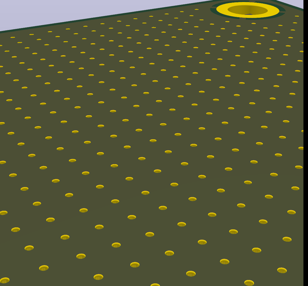
The 1,076 vias placed live in KiCad:
Going further
For a simple grid without exclusions, see the stitching via grid. To check the result, count the vias per net, then run the DRC with headless kicad-cli.